Application Hints for the Hybrid Cascode IF Amplifier
18Nov07, update 21Nov, 2Dec, 6Dec07, 2Jan08.
Modifications (Some of these
things are now included in the errata.)
1. We have added two outputs to the board layout that are not
detailed in the QST article. The first output is a DC signal
that is merely the AGC voltage. A resistor (R37, value = 10K) is
added to the board just to protect the AGC line from any loading that might
appear on the line. The intended purpose of this voltage is to drive
an S-Meter. A driver circuit is presented below. The
second added output is the 9 volt output from the regulator on the IF board.
This voltage is used as a reference for the S-Meter driver.
It also may be handy as a supply for an oscillator elsewhere in the
design that might use the IF system.
2. The input inductor, L1, is dropped from 7.2 to 6.8 uH.
A toroid can be wound, or an RF Choke can be dropped into this slot.
This L should have a Q of 40 or higher for best match and noise figure.
3. The value of resistor R7 is decreased from 3.3K to 3.0K.
This is the impedance that fits with the 6.8 uH at 9 MHz.
4. R15 changes from 3.3K to 3.0K. If you want
slightly higher gain, you can use 3.3K.
5. Inductors L2, L3, and L4 are replaced with 47 uH RF
Chokes. This keeps the costs down and eliminates the need
to wind some toroids. There is one left, and the builder must wind
this. No, Roger won't do it for you!
6. Add an 18 Ohm resistor, R38, in series with C12, which
connects the emitters of Q7 and Q8. For
details, click here.
7. External threshold control: Jeff, WA7MLH,
liked the behavior of the system when he adjusted R6 on the test bench, so
he ended up with a front panel pot for the control. This variation
might be one to consider in some experimental receivers.
An S-Meter Driver for the Hybrid Cascode Hybrid IF Amplifier
Many receiver builders planning on using the Hybrid Cascode IF amplifier
will want to incorporate an S-Meter in their design. We have designed
a circuit that should provide a good start for the design.
Two curves are presented here for the closed loop AGC system response.
This is a curve of detected DC appearing on the "AGC line"
(emitter of Q9) versus the signals applied to the input. This particular
curve was generated with a ferrite input transformer driving Q2.
(Note: The curve shown was taken with an earlier
version of the IF amplifier with slightly different biasing voltages for
the manual gain control, so the voltages are different. The maximum
AGC voltage is 5.5 in the curve. The max is about 7.3 volts in the
QST design. )
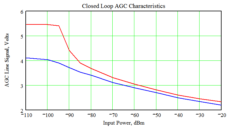
The red curve represents a relatively high AGC threshold. This
is the "ear-saver" kind of characteristic that I personally prefer for
casual operation. The receiver sounds as if there is no AGC in the
system at all until the input to the AGC amplifier is -95 dBm. The
AGC loop then begins to reduce the IF gain as the signals become stronger.
R6 is short circuited for the red curve. The blue curve
is the one obtained with R6 (threshold) at 270 Ohms. This
is more in line with the kind of AGC that we find in many commercial radios
where the noise within the radio is already enough to turn the AGC on.
The radio output never gets too loud and all signals sound
the same. It also yields an S-meter response that begins
at low levels. The builder/experimenter needs to make a choice
and set R6 accordingly. Some experimenters are
using a pot for R6.
Looking at the curves, we see that a "no signal" input to an S-Meter
driver circuit may be as high as 5.5 volts. It will drop toward
2 volts as signals become very large. This gives us something
to use for design.
A suitable circuit is shown below. This is an updated version (6 Dec 07) of the original, designed for ease
of adjustment and compatibility with about any version of the AGC that a
builder might generate.
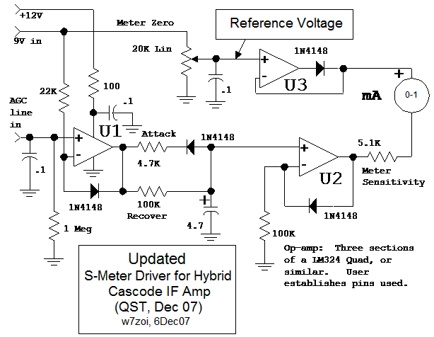
Three connections are required to the outside world (plus ground.)
The first is the 12 volt supply that is usually in the
receiver. This can go much higher. The IF amplifier itself
assumes that the supply never drops below 11 volts. If a lower
voltage is expected, redesign is in order, perhaps with a low dropout regulator.
We used a modest LM317L in the IF. The second connection
is to the 9 volt signal that is generated within the IF. We
used this as a reference in the driver circuit, but do not ask much more
than a couple of mA of current from it. The third input needed
is, of course, the AGC signal itself. This is the voltage predicted
by the curve above. The signal marked "Reference Voltage" should
equal the voltage on the AGC bus with zero signal into the amplifier and
with the manual gain control at maximum. This is a little over 7 volts
for the amplifiers we have built in the last couple of months.
U1 is nothing more than a high input impedance buffer. It has
a diode of downward offset in the output. This merely compensates
for the offset in the diode that follows the op-amp. The circuit
that follows is a diode network that allows the meter to attack quickly,
but be damped so far as the recovery is concerned. I believe
that this general scheme can be attributed to Bill Sabin. The various
resistors are marked with regard to function. The voltage on
the damping capacitor drives U2, another non inverting buffer which is the
meter driver.
Op-amp U3 is a "perfect" rectifier. It provides a stable
"floating ground" to deflect the meter against, but it does not allow any
deflection in the wrong direction. The overall system is configured
to drive a 1 mA meter movement, which is very common. If a
more sensitive meter is used, the meter deflection resistor (5.1K) can be
increased accordingly. For example, if a 100 uA movement is used,
the resistor would become 51K. If a less sensitive meter is
to be used, emitter followers may be required in the output of U2 and U3.
They should be within the feedback loops. The S-meter
is adjusted to zero with the pot when the antenna is disconnected from
the receiver.
I have NOT built this circuit. However, it should provide a
reasonable start for developing a circuit for a specific application.
Feedback: The first version of
this circuit was posted on November 18th. I got a note on Nov 21
from K4ZKU and Jeff said that he had breadboarded it and had it working
with an earlier IF amplifier (probably from the Progressive Receiver) and
that it worked fine. Many thanks Jeff. The newer
version shown above is actually a simpler and less interactive design.
The version shown above was first built by John, K5IRK. Jeff, WA7MLH
also has a version running now. No problems reported with either.
Many thanks to both.
Shielding
Jeff Damm, WA7MLH, had some interesting observations after he dropped one
of these IF amplifiers into one of his homebrew SSB transceivers.
He had built the S-Meter driver earlier and had it operating with
the IF amplifier. But he noted that the S-Meter was partially on when
the board was in the transceiver. He had no shielding on the
IF, and some of the other modules were also open. Jeff discovered
that the problem was direct signal pick-up from part of his LO system.
As soon as the board was removed, but still electrically attached to the
transceiver, the problem disappeared. A shield is now
planned for the transceiver.
Input Crystal Filter Considerations
The input to the hybrid cascode amplifier is shown below.
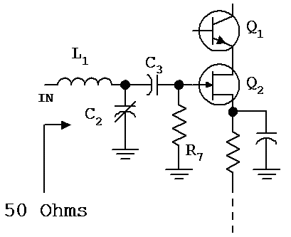 With no gain reduction, the current in the two transistors is about
3 mA with the biasing used in the QST design. The input impedance
seen looking into Q2 is very high, but with some shunt capacitance.
The net input impedance when looking into R7 is just the value of
R7 paralleled with a few pF. R7 was 3.3K in our design.
With no gain reduction, the current in the two transistors is about
3 mA with the biasing used in the QST design. The input impedance
seen looking into Q2 is very high, but with some shunt capacitance.
The net input impedance when looking into R7 is just the value of
R7 paralleled with a few pF. R7 was 3.3K in our design.
The most convenient topology for many applications is one with a 50
Ohm input impedance. (It is the most easily measured, which
is a useful criterion in a homebrew receiver.) C3 is merely
a blocking capacitor and can be ignored. The 3.3K is transformed
down to 50 Ohms with a simple L-network. The design formula for this
is in virtually every Handbook or RF design manual that has appeared for
nearly a century. We did not merely present a reactance with
the components, for the builder may wish to change the value of R7 to decrease
or increase the overall gain.
Many classic IF systems drive a high impedance (a FET or IC) with
the output of a crystal filter. The filter must be properly
terminated to achieve the desired design shape. A common
termination is 500 Ohms. It is common to replace R7 above
with a 510 Ohm resistor, dispense with L1 and C2, and drive C3 directly
with the crystal filter. This works fine. However,
you loose some gain with this procedure. The higher termination resistance
leads to higher gain. One could design an L-network to transform from
500 Ohms up to 3300 Ohms. This is shown below.
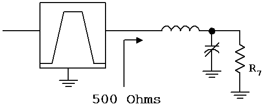 The builder can design the network to suit his or her application.
Another alternative would be to use an L-network (or some other transforming
circuit) to drop from 500 Ohms to 50 Ohms and to then go into a shielded
IF amplifier box with coaxial cable to a higher impedance such as our 3.3K.
This is presented below.
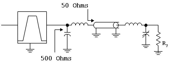 This is probably the scheme I would use when designing
a new receiver or transceiver. The Hybrid Cascode circuit
was configured to allow experimental flexibility.
This is probably the scheme I would use when designing
a new receiver or transceiver. The Hybrid Cascode circuit
was configured to allow experimental flexibility.
Output Level Programming, including a Noise Filter Interface
The output network is also configured for flexibility. The
present circuit is shown here:
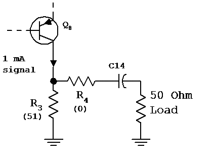 R3 is normally set to 51 Ohms while R4 is a short circuit.
C14 is again just a blocking capacitor and has no impact on performance.
This configuration then presents a 50 Ohm output impedance,
for the impedance looking back into the Q8 collector is very high.
The 50 Ohm load, which might be a diode ring product detector, is then
properly driven. The impedance is proper on a wideband basis
and the level is low enough for low distortion.
R3 is normally set to 51 Ohms while R4 is a short circuit.
C14 is again just a blocking capacitor and has no impact on performance.
This configuration then presents a 50 Ohm output impedance,
for the impedance looking back into the Q8 collector is very high.
The 50 Ohm load, which might be a diode ring product detector, is then
properly driven. The impedance is proper on a wideband basis
and the level is low enough for low distortion.
The output from Q8 above is labeled with a "1 mA signal" current.
This is NOT the level present. Rather, it is a hypothetical
level we picked for some later calculations. Let's examine
this case with 1 mA. This signal is presented to a net impedance
of 25 Ohms, which is the parallel combination of the 50 Ohm load and R3.
With a 1 mA signal, Ohm's Law tells us that the signal voltage at
the load is 25 mV. This appears across the 50 Ohm load, so the power
delivered to the load is 12.5 microwatts, or .0125 milliwatt, which converts
to -19 dBm.
One might wish to drive other product detectors. One
could probably get reasonable performance with a NE602 or similar low
current Gilbert cell by terminating the detector input with a 51 Ohm resistor.
On the other hand, if a transformer was used to drive the input of
that cell, the drive might be excessive, leading to distortion.
I observed this with a transceiver built many years ago and only
fixed it when a 20 dB pad was inserted ahead of the detector. It
all depends on the exact signal voltages.
The Hybrid cascode was configured to allow the user to drop the levels.
Here's an example of such an application.
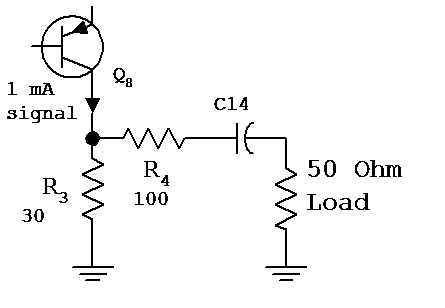 We have decreased the resistor R3, which forces the signal
voltage to a lower level. R4 was changed to 100 Ohms.
The net load at the collector is now 150 Ohms in parallel with R3,
which is again 25 Ohms. The 1 mA signal will then generate
the same 25 mV at the collector. This will cause a signal current
to flow into the 150 Ohm arm of 0.167 mA. The voltage across
the 50 Ohm load is then 8.333 mV. The corresponding power is
1.39 microwatt, or .00139 mW. This corresponds to a level
of -28.6 dBm. The circuit change has attenuated the output
by 9.6 dB. The output is no longer matched. It
would be possible to retain a matched output if the sum of R3 and R4 was
50 Ohms.
We have decreased the resistor R3, which forces the signal
voltage to a lower level. R4 was changed to 100 Ohms.
The net load at the collector is now 150 Ohms in parallel with R3,
which is again 25 Ohms. The 1 mA signal will then generate
the same 25 mV at the collector. This will cause a signal current
to flow into the 150 Ohm arm of 0.167 mA. The voltage across
the 50 Ohm load is then 8.333 mV. The corresponding power is
1.39 microwatt, or .00139 mW. This corresponds to a level
of -28.6 dBm. The circuit change has attenuated the output
by 9.6 dB. The output is no longer matched. It
would be possible to retain a matched output if the sum of R3 and R4 was
50 Ohms.
In some cases it is desired to place a crystal noise filter at the
output of the IF amplifier, prior to the product detector. If
we were again using a 500 Ohm filter, the noise filter could be properly
matched if R3 was changed to 510 Ohms. This is shown below.
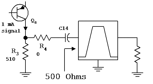 This circuit uses a higher termination at the collector
of Q8. Hence, the gain will be higher by 10 dB. We will
leave it to the reader to demonstrate this.
This circuit uses a higher termination at the collector
of Q8. Hence, the gain will be higher by 10 dB. We will
leave it to the reader to demonstrate this.