Bypass and Decoupling
Capacitors--Some Thoughts and Modeling
Wes Hayward, w7zoi 4 Sept 2019.
A recent on-line post asked about the practices that we used with
circuits in the book Experimental Methods in RF Design.
The question asked about the decoupling resistors used and how the
values were determined. This is a subject that I often
encounter and I thought it would be worth further
discussion.
Let's start with a common circuit, a two stage
amplifier. Both stages are identical, but the
component values are usually different. There is
nothing special about this circuit. It's just a vehicle for
our discussion.
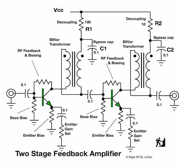 Fig 1. Each of the
two stages in this circuit is decoupled from the power source with
a resistor. R1 is 100 and R2=10 ohms. The two
stages each have power gain, so the signals at the input to the
second stage are larger than those at the input to the first
stage. The second stage will probably be biased for
more current, so that decoupling resistor, R2, must be
lower. The decoupling element is part of
the overall bias and must be taken into account during bias
design.
Fig 1. Each of the
two stages in this circuit is decoupled from the power source with
a resistor. R1 is 100 and R2=10 ohms. The two
stages each have power gain, so the signals at the input to the
second stage are larger than those at the input to the first
stage. The second stage will probably be biased for
more current, so that decoupling resistor, R2, must be
lower. The decoupling element is part of
the overall bias and must be taken into account during bias
design.
Let's back away from the application shown in Fig 1 and
concentrate on just one stage, and specifically, on one of the
bypass capacitors, C1. The value for this part is 0.1
uF, certainly a popular and common part. This
component has two functions. First, as a bypass, it
establishes the AC potential at zero. The capacitor
will, of course, have a DC present from the bias, but will force
the AC signal voltage toward zero. Recall that a
capacitor is an element that resists a change in voltage, just as
an inductor impedes a change in current.
Assume that capacitor C1 is perfect. We'll discuss
imperfections later. So, how effective is C1 in
attenuating noise or signals that might be on the power supply
buss, assuming no decoupling resistor? The
power supply is not perfect. That is, it has a finite
output impedance that may well be a function of
frequency. Assume for this example that
the power supply has an output resistance of 1
ohm. The behavior of C1 is then
shown in Fig. 2 below, a SPICE calculation of the response of the
filter formed by the 1 ohm power supply resistance and
C1.
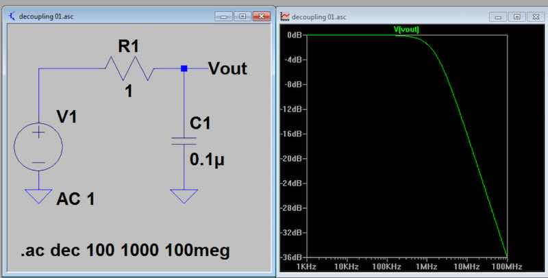 Fig 2. This circuit produces the
response in the related curve. The response can be
used to calculate the impedance (magnitude) of the capacitor
versus frequency.
Fig 2. This circuit produces the
response in the related curve. The response can be
used to calculate the impedance (magnitude) of the capacitor
versus frequency.
The reactance of the 0.1 uF capacitor can be calculated
directly. This is shown in the following table.
F
Xc
1 kHz 1591 ohm
1 MHz 1.59
10 MHz 0.16
100 MHz .016
What happens if we now include 10 or 100 ohm
resistors? These are compared with the 1 ohm
response in Fig 3.
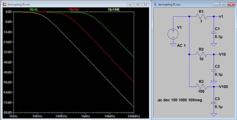 Fig 3. Response with various values of
resistance in the single element low pass filter. (It
is just a single filter that is analyzed three
times.) A change in R by 10 yields a 20 dB
improvement in attenuation of power supply noise at the
capacitor. C1 is assumed to be perfect. Note
that all three plots have the same slope of 6 dB/octave or 20 dB
per decade.
Fig 3. Response with various values of
resistance in the single element low pass filter. (It
is just a single filter that is analyzed three
times.) A change in R by 10 yields a 20 dB
improvement in attenuation of power supply noise at the
capacitor. C1 is assumed to be perfect. Note
that all three plots have the same slope of 6 dB/octave or 20 dB
per decade.
Now for some reality. If a capacitor is studied with a
network analyzer, a strong resonance is observed in almost all
cases. This is the result of so called lead
length inductance resonating with the
capacitance. The term lead length is
something of a misnomer, for even SMT parts with zero lead length
will show this resonance. As it turns out, all
that is required to obtain an effective inductance is the physical
length of the capacitor.
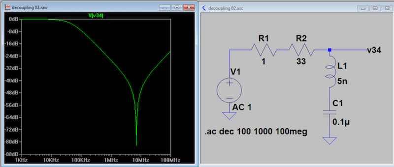 Fig 4. This plot models the capacitor
as a series LC where the C is the low frequency measured value of
0.1 uF and the L is commensurate with the length. A
reasonable inductance constant is 10 nH/cm. The best
way to get the L parameter though is to measure it.
Measure the resonant frequency and calculate L on the basis of the
marked capacitance. (Remember Kopski's rule:
TMITK, or "To Measure is to Know.) This example
uses a 33 ohm decoupling resistor. The slope of the
response and the frequency where it starts to depart from the zero
attenuation by a dB or so are the same as the the earlier examples
when R is taken into account. The resonance for
this example is 7 MHz.
Fig 4. This plot models the capacitor
as a series LC where the C is the low frequency measured value of
0.1 uF and the L is commensurate with the length. A
reasonable inductance constant is 10 nH/cm. The best
way to get the L parameter though is to measure it.
Measure the resonant frequency and calculate L on the basis of the
marked capacitance. (Remember Kopski's rule:
TMITK, or "To Measure is to Know.) This example
uses a 33 ohm decoupling resistor. The slope of the
response and the frequency where it starts to depart from the zero
attenuation by a dB or so are the same as the the earlier examples
when R is taken into account. The resonance for
this example is 7 MHz.
There is some virtue to this resonance. There are some
applications where it is desirable to get a very good bypass or
good decoupling at one specific frequency.
However, in most cases, we want good wide band performance.
The previous example used a 0.1 uF capacitor with a stray L of 5
nH. The next example considers a 1000 pF
capacitance with stray L of 2 nH.
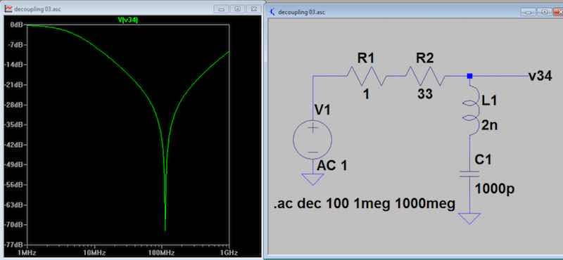 Fig
5. The frequency sweep is repeated, but over a
wider bandwidth. This part resonates at 114
MHz. The response away from the dip is like the
simpler parts.
Fig
5. The frequency sweep is repeated, but over a
wider bandwidth. This part resonates at 114
MHz. The response away from the dip is like the
simpler parts.
This is where things get embarrassing: Back in
the 1970s, lore among RF folks was that a good way to enhance wide
band decoupling was to use parallel capacitors of differing
value. Combinations of 3 or more were common, with a
common set being 0.1 uF, .01 uF, and 1000 pF.
Sometimes additional parts were added. The
following Fig 6 shows what happens with the parallel combination
of a 0.1 uF and 1000 pF, the two capacitors just analyzed.
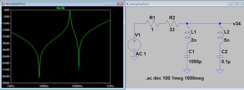 Fig 6. A second tuned LC is added to the first bypass
capacitor, generating the predicted second dip. The
overall response values are -82 dB at 7 and -72 dB at 112
MHz. But there is a major problem: the
attenuation is less than 1 dB at 60 MHz! This could
be a really big problem in some circuits. At that
frequency, there is virtually no decoupling or bypassing at
all. The circuit using this quasi bypass would
operate as if there was no bypass at all at that frequency.
How many cases of stray oscillation can be explained
by this; I can think of some. Note that parallel
resonance happens where the 1000 pF resonates with the total L of
both elements, 7 nH.
Fig 6. A second tuned LC is added to the first bypass
capacitor, generating the predicted second dip. The
overall response values are -82 dB at 7 and -72 dB at 112
MHz. But there is a major problem: the
attenuation is less than 1 dB at 60 MHz! This could
be a really big problem in some circuits. At that
frequency, there is virtually no decoupling or bypassing at
all. The circuit using this quasi bypass would
operate as if there was no bypass at all at that frequency.
How many cases of stray oscillation can be explained
by this; I can think of some. Note that parallel
resonance happens where the 1000 pF resonates with the total L of
both elements, 7 nH.
Embarrassment was mentioned above. In my 1982 book,
Introduction to RF Design (Prentice-Hall, 1982), page
13, I repeated the lore of the day regarding the parallel unequal
capacitors. Clearly, this was an error. I had
completely forgotten about this statement. I do
remember colleagues blowing a hole in this lore sometime at about
1990 when I was working at TriQuint Semiconductor.
The next example adds one more capacitor to the mix, a .01 uF with
stray L of 3 nH.
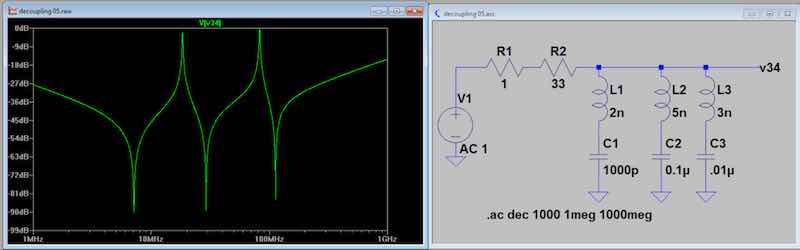 Fig 7. Three capacitors are paralleled to produce
three series frequencies of high attenuation, but two undesired
intermediate frequencies of almost no
filtering.
Fig 7. Three capacitors are paralleled to produce
three series frequencies of high attenuation, but two undesired
intermediate frequencies of almost no
filtering.
When Rick Campbell and Bob Larkin and I were putting Experimental
Methods in RF Design (ARRL, 2003) together, I
started to write the same old lore. It had been around
so long that I started to believe it. But
Bob caught it. Moreover, he was experienced in these
things and knew to point me in a direction that actually
works. Figure 8 below shows what happens when
three capacitors of EQUAL value are used for a bypass. In
this case, three .01 uF caps, each with L=3 nH are paralleled.
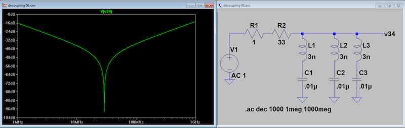 Fig
8. Three identical capacitors produce a very deep null at
resonance, but do not generate an offensive parallel
resonance.
Fig
8. Three identical capacitors produce a very deep null at
resonance, but do not generate an offensive parallel
resonance.
It only gets better as more capacitors are added. The
figure below shows the response with 7 identical parallel
capacitors.
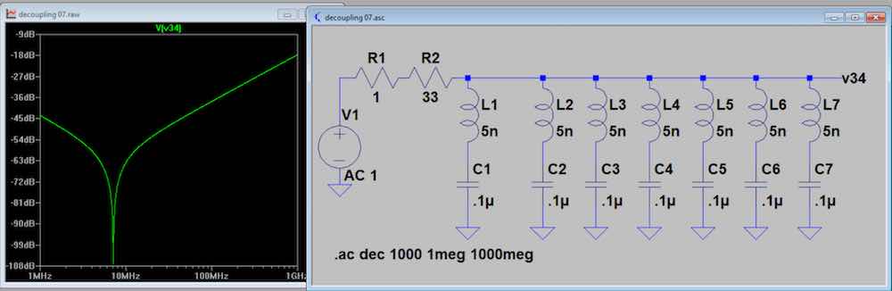 Fig 9. This example is much like the
previous case, but the .01 uF caps are replaced by seven
0.1 uF units with 5 nH stray L. Again, no stray parallel
responses are seen.
Fig 9. This example is much like the
previous case, but the .01 uF caps are replaced by seven
0.1 uF units with 5 nH stray L. Again, no stray parallel
responses are seen.
We often see designs where stages are bypassed, but there is no
decoupling. That is, R1 and R2 of Fig 1 are
eliminated. Sometimes the circuit works, but
sometimes it does not and there may be no obvious
reason. The following
schematic illustrates this. When the amplifiers
of Fig 1 uses no decoupling resistors, the two 0.1 uF bypass caps
are then paralleled, resulting in the 0.2 uF capacitor of Fig
10. The increased C value has little
impact. The larger problem, one that has major
impact is that the two stages are now tightly coupled to each
other. Any signal at one amplifier might
generate a voltage across the bypass. But that signal
is now available, without attenuation, to the bypass capacitor
node of the other stage. After all, those two
nodes are one and the same. The problem is potentially even
worse. C1 of Fig 1 spans from the
transformer power supply end to ground. The same
argument applies to C2 in the second stage of Fig 1.
The grounds are different. They may even be in
different shielded enclosures. When
the decoupling resistors disappear, the two capacitors become one
and all ground signals in one stage are now shared with the other.
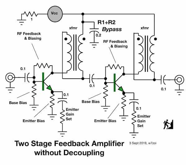 Fig 10. This circuit illustrates
the problem sometimes encountered when decoupling resistor for
each stage are eliminated.
Fig 10. This circuit illustrates
the problem sometimes encountered when decoupling resistor for
each stage are eliminated.
We should elaborate by what is intended when we say that a design
"does not work." In the extreme, there may be an
oscillation, an obvious problem. But the more common
dysfunction is more subtle. The gain may be more or less
than we sought in our design. This can be especially
frustrating in measurement equipment. Even more
insidious, the distortion may be out of line. It is
important in a careful design to simulate these things and then to
measure them and compare the results.
The analysis so far has examined the signal (or noise) from the
power supply that might end up at one of the amplifier
stages. The decoupling also operates
in the other direction. Envision Fig 1 where a
signal source is now placed in parallel with C1. This
emulates a signal that may be in the first stage. A small
resistance (R1, below) is included with the source.
Voltage sources don't play well with lossless reactive
terminations in SPICE. We wish to evaluate the
strength of this signal when it reaches the supply.
The power supply itself serves as a load for this
signal. This analysis is shown in Fig 11 below.
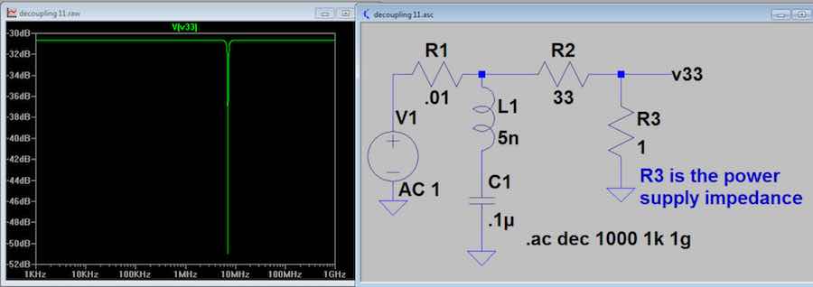 Fig 11. A 33 ohm
decoupling resistor acts against the power supply internal 1 ohm
impedance to provide a 31 dB attenuation at the supply for signals
originating within the amplifier. Dropping
the decoupling R to 5 ohms reduces the attenuation to 16 dB.
Fig 11. A 33 ohm
decoupling resistor acts against the power supply internal 1 ohm
impedance to provide a 31 dB attenuation at the supply for signals
originating within the amplifier. Dropping
the decoupling R to 5 ohms reduces the attenuation to 16 dB.
Loss can alter the results. This is easily modeled
with the insertion of series resistance in the "capacitor" series
LC model.
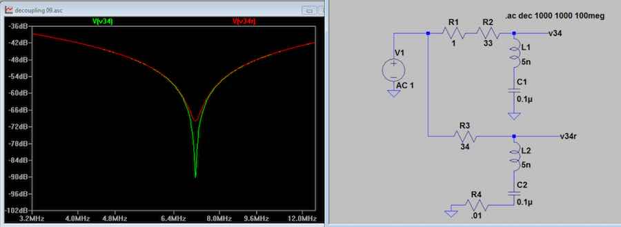 Fig 12. This plot is just a repeat of Fig 4
except that a second circuit variant is added that includes a .01
ohm series resistance. That response is shown in
red. Loss has minimal impact except when
examining the depth of the notch related to the capacitor series
resonance.
Fig 12. This plot is just a repeat of Fig 4
except that a second circuit variant is added that includes a .01
ohm series resistance. That response is shown in
red. Loss has minimal impact except when
examining the depth of the notch related to the capacitor series
resonance.
Quite a bit of discussion has been devoted to the use of parallel
capacitors. A rule emerges--only use them when
the caps are of equal value. One possible exception to the
recommendation to avoid unequal caps has to do with an added
electrolytic capacitor. In one experiment, I had
measured a filtering decoupling network, much like Fig 4, and then
added a 100 uF aluminum electrolytic. It was nothing
special, but just one of the routine parts that we
use. The measurement was
repeated. The performance at RF changed by no
more than 1 dB over the HF band of interest. The low
frequency decoupling was improved.
Concluding Thoughts
Any stage in a system, be it a transmitter, a receiver, or a
complete transceiver, will have several stages.
These will all require at least one bypass capacitor.
Often, the bypass is also part of a decoupling network that routes
to a power supply or a control signal. A viable
rule is that a bypass for one stage should never be shared
with a second stage. Moreover. each line that leave
the stage should be through an impedance. If a
resistor is not desired, an RFC can sometimes be used.
Sometime it is necessary to join several of these supply lines
together in a bypass capacitor. An example might be a
feed through capacitor where several stage within a shielded
enclosure reside. It may then be useful to add an
impedance after the common shunt capacitor.
I've often done transceivers where the only stage that is
connected directly to the power supply is the output power
amplifier. Every other stage attaches to the power
supply with a series impedance.
There is a school of folks who will build a rig, and will then
start removing parts with the hope that the rig will continue to
function. I don't embrace this approach.
Finally, it is interesting to look at an exercise like the one I
just went through and to attribute it to our modern
conveniences. We all have some reasonable measurement
equipment, with a 50 MHz oscilloscope as a
minimum. And we all have a compute with free
software that does all sorts of interesting, fun stuff for
us. I used LT SPICE for this effort.
(Thanks to Linear Technology, now part of Analog
Devices.) But none of this analysis required any
of this sophistication. All analysis was linear and
could be done with a programmable hand calculator.
Indeed, it could probably have been done with paper and slide
rule, although it would get pretty tedious.